More Option
XCZU49DR-2FFVF1760I Multi-Channel RF-ADC/DAC Data Disorder and No-Output Troubleshooting Guide for Zynq UltraScale+ RFSoC
BY: GALAXY
2 hours ago
 Applicable Device
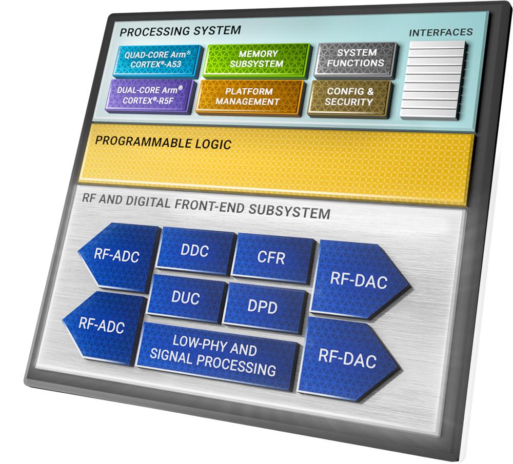
XCZU49DR-2FFVF1760I (Zynq UltraScale+ RFSoC)
Typical Applications
- Phased-Array Radar
- 5G Radio Units (RU)
- Satellite Communications
- Software-Defined Radio (SDR)
- High-Speed Test & Measurement Systems
- Multi-Channel Synchronous Transceiver Platforms
Typical Symptoms
When operating a single ADC/DAC channel, the system functions normally. However, during multi-channel synchronous operation, the following issues may occur:
- Data disorder or out-of-sequence samples
- Sampling misalignment
- Phase inconsistency among channels
- No output from certain channels
- Random packet or sample loss
1. Problem Overview
Multi-channel ADC/DAC abnormalities on the XCZU49DR RFSoC are rarely caused by silicon defects. Most failures originate from improper Multi-Tile Synchronization (MTS) configuration, inadequate clock quality, JESD204B link parameter mismatches, insufficient power integrity, or PCB signal integrity issues.
This article provides a concise troubleshooting workflow and proven corrective actions that can be directly applied during RFSoC project debugging and validation.
2. Five Common Root Causes
1. Missing Multi-Tile Synchronization (Highest Probability)
The RFSoC architecture contains multiple independent ADC and DAC tiles. Without proper synchronization, channels may experience:
- Sample misalignment
- Data disorder
- Frame loss
- Phase drift
Common causes include:
- MTS/MCS not enabled
- SYSREF constraints not configured
- Missing channel phase calibration
2. RFDC IP or Driver Configuration Errors
Configuration mismatches can disrupt data transmission and decoding, including:
- JESD204B line rate mismatch
- Incorrect lane configuration
- Sampling rate inconsistency
- Device tree SYSREF configuration errors
- Incorrect channel ID assignments
- AXI data width alignment issues
These issues frequently result in channel failures, corrupted data, or unexpected behavior.
3. Clock and Power Quality Issues
Stable RFSoC operation depends heavily on clock and power integrity.
Common problems include:
- Excessive REFCLK jitter
- Frequency offset beyond specification
- SYSREF skew between tiles
- Poor SYSREF edge quality
- Excessive analog power ripple
- Digital-to-analog ground coupling noise
These conditions may cause unstable sampling performance and intermittent channel failures.
4. PCB Signal Integrity Problems
PCB implementation can significantly impact multi-channel performance.
Typical issues include:
- Excessive RF trace length mismatch
- Improper JESD204B differential impedance control
- Missing or discontinuous reference planes
- Insufficient power decoupling
Consequences often include:
- Link packet loss
- Phase inconsistency
- Elevated operating temperature
- Reduced system reliability
5. RF Front-End Hardware Issues
Hardware-level defects can directly affect channel output.
Examples include:
- Poor solder joints
- Damaged RF front-end components
- DAC output buffer disabled
- Load impedance mismatch
These problems may lead to waveform distortion or complete channel output failure.
3. Standardized Troubleshooting Procedure
Troubleshooting Principle
Single Channel → Multi-Channel
Software → Hardware
Configuration → Physical Inspection
Step 1: Verify Single-Channel Operation
Enable only one ADC/DAC channel for testing.
If the channel operates normally:
- RFSoC silicon is likely functional
- Power rails are generally healthy
- Front-end hardware is likely intact
Focus troubleshooting on:
- Multi-channel synchronization
- JESD204B configuration
- Timing alignment
If single-channel operation also fails, investigate:
- Power supplies
- Clock sources
- Soldering quality
- Hardware assembly
Step 2: Correct Multi-Channel Synchronization Settings (Critical Step)
Recommended actions:
- Enable RFDC MTS/MCS synchronization
- Configure SYSREF pulse mode
- Apply proper timing constraints
- Bind all channel IDs in the device tree
- Execute link alignment procedures
- Calibrate path delay
- Perform NCO phase calibration
Step 3: Validate Clock and Power Parameters
Recommended targets:
| Parameter | Recommendation |
|---|---|
| REFCLK Jitter | Ultra-low jitter source |
| Frequency Accuracy | ≤ ±1 ppm |
| SYSREF Skew Between Tiles | ≤ 50 ps |
| Analog Power Ripple | ≤ 10 mVpp |
| Grounding Strategy | Single-point analog/digital grounding |
Step 4: Verify JESD204B Link Status
Ensure consistency between RFDC IP and transceiver settings.
Recommended checks:
- JESD204B lane configuration
- Line rate settings
- Frame alignment status
- SYNC status
- CRC error counters
Use Integrated Logic Analyzer (ILA) tools to monitor link health and verify stable operation without packet loss.
Step 5: Inspect PCB and RF Front-End Hardware
Recommended design targets:
- RF trace length mismatch ≤ 5 mil
- Differential impedance controlled at 100 Ω
- Adequate high-speed reference planes
- Sufficient power decoupling
Hardware checks:
- RF component soldering quality
- DAC output buffer configuration
- Load impedance matching
4. Typical Failure Cases and Solutions
Case 1: Data Disorder and Phase Offset
Root Cause
- MTS synchronization disabled
- SYSREF timing constraints missing
Solution
- Enable MTS/MCS synchronization
- Add SYSREF timing constraints
- Perform phase calibration
Result
Stable channel alignment and synchronized operation restored.
Case 2: Random No Output and High-Temperature Failures
Root Cause
- Excessive clock jitter
- Poor power decoupling
Solution
- Replace with a low-jitter oscillator
- Optimize power distribution network (PDN)
Result
Reliable operation across both high- and low-temperature environments.
Case 3: DAC Channel No Output
Root Cause
- Output buffer disabled
- Load impedance mismatch
Solution
- Enable DAC output buffer
- Match output load impedance
Result
Normal waveform output restored.
5. Best Practices for Reliable Deployment
1. Prioritize Synchronization Architecture
For all multi-channel array systems, MTS/MCS synchronization and SYSREF timing constraints should be considered mandatory design requirements.
2. Build a Solid Hardware Foundation
System reliability starts with:
- Low-jitter clock architecture
- Low-ripple power supplies
- Proper PCB layout practices
These measures prevent many issues before they occur.
3. Follow a Structured Debug Flow
Always use the sequence:
Single-Channel Testing → Multi-Channel Configuration → Full-System Integration
This approach significantly reduces troubleshooting time.
4. Reserve Calibration Interfaces
Include amplitude and phase calibration mechanisms during system design to ensure manufacturing consistency and long-term performance.
6. Product Supply and Technical Support
We maintain inventory of the XCZU49DR-2FFVF1760I RFSoC, offering:
- Genuine original devices
- Ready stock availability
- Sample support
- Fast delivery
- Long-term supply agreements
In addition, we provide comprehensive technical support services, including:
- Standard RFDC configuration templates
- Timing constraint scripts
- Multi-channel synchronization solutions
- PCB design guidance
- On-site debugging assistance
These resources help accelerate RFSoC development and reduce project deployment risk.


Home
Center